- 您现在的位置:买卖IC网 > Sheet目录983 > HI5662EVAL2 (Intersil)EVALUATION PLATFORM HI5662
�� �
�
�Application� Note� 9823�
�Appendix� D� HI5662� A/D� Theory� of� Operation�
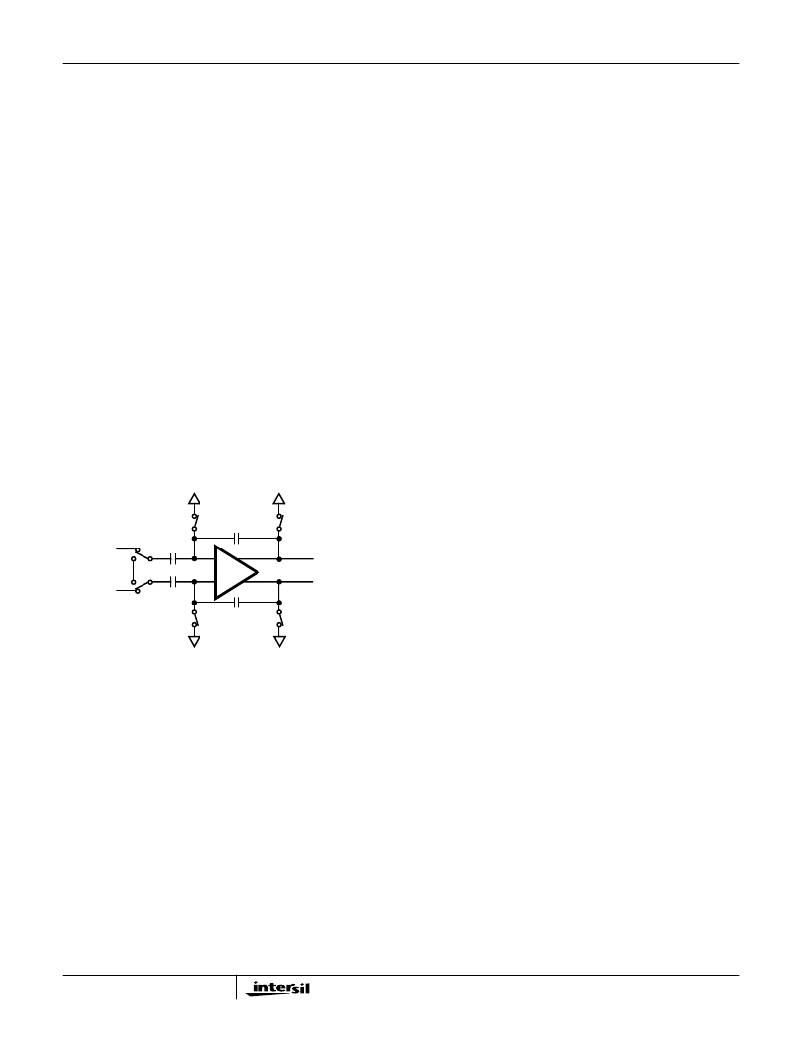
�The� HI5662� is� a� dual� 8-bit� fully� differential� sampling� pipeline�
�A/D� converter� with� digital� error� correction� logic.� Figure� 22�
�depicts� the� circuit� for� the� front� end� differential-in-differential-�
�out� sample-and-hold� (S/H)� amplifiers.� The� switches� are�
�controlled� by� an� internal� sampling� clock� which� is� a� non-�
�overlapping� two� phase� signal� ,� Φ� 1� and� Φ� 2� ,� derived� from� the�
�master� sampling� clock.� During� the� sampling� phase,� Φ� 1� ,� the�
�input� signal� is� applied� to� the� sampling� capacitors,� C� S� .� At� the�
�same� time� the� holding� capacitors,� C� H� ,� are� discharged� to�
�analog� ground.� At� the� falling� edge� of� Φ� 1� the� input� signal� is�
�sampled� on� the� bottom� plates� of� the� sampling� capacitors.� In�
�the� next� clock� phase,� Φ� 2� ,� the� two� bottom� plates� of� the�
�sampling� capacitors� are� connected� together� and� the� holding�
�capacitors� are� switched� to� the� op-amp� output� nodes.� The�
�charge� then� redistributes� between� C� S� and� C� H� completing� one�
�sample-and-hold� cycle.� The� front� end� sample-and-hold� output�
�is� a� fully-differential,� sampled-data� representation� of� the�
�analog� input.� The� circuit� not� only� performs� the� sample-and-�
�hold� function� but� will� also� convert� a� single-ended� input� to� a�
�fully-differential� output� for� the� converter� core.� During� the�
�sampling� phase,� the� I/Q� IN� pins� see� only� the� on-resistance� of� a�
�switch� and� C� S� .� The� relatively� small� values� of� these�
�components� result� in� a� typical� full� power� input� bandwidth� of�
�250MHz� for� the� converter.�
�digital� delay� line� is� to� time� align� the� digital� outputs� of� the� eight�
�identical� two-bit� subconverter� stages� with� the� corresponding�
�output� of� the� ninth� stage� flash� converter� before� applying� the�
�eighteen� bit� result� to� the� digital� error� correction� logic.� The�
�digital� error� correction� logic� uses� the� supplementary� bits� to�
�correct� any� error� that� may� exist� before� generating� the� final�
�eight� bit� digital� data� output� of� the� converter.�
�Because� of� the� pipeline� nature� of� this� converter,� the� digital�
�data� representing� an� analog� input� sample� is� output� to� the�
�digital� data� bus� following� the� 6th� cycle� of� the� clock� after� the�
�analog� sample� is� taken� (see� the� timing� diagram� in�
�Figure� 24).� This� time� delay� is� speci?ed� as� the� data� latency.�
�After� the� data� latency� time,� the� digital� data� representing�
�each� succeeding� analog� sample� is� output� during� the�
�following� clock� cycle.� The� digital� output� data� is� provided� in�
�offset� binary� format.�
�Internal� Reference� Voltage� Output,� V� REFOUT�
�The� HI5662� is� equipped� with� an� internal� reference� voltage�
�generator,� therefore,� no� external� reference� voltage� is� required.�
�V� ROUT� must� be� connected� to� V� RIN� when� using� the� internal�
�reference� voltage.�
�An� internal� band-gap� reference� voltage� followed� by� an�
�amplifier/buffer� generates� the� precision� +2.5V� reference�
�voltage� used� by� the� converter.� A� band-gap� reference� circuit�
�I/Q� IN+�
�I/Q� IN-�
�Φ� 1�
�Φ� 2�
�Φ� 1�
�Φ� 1�
�C� S�
�C� S�
�Φ� 1�
�C� H�
�-� +�
�+� -�
�C� H�
�Φ� 1�
�Φ� 1�
�V� OUT+�
�V� OUT-�
�is� used� to� generate� a� precision� +1.25V� internal� reference�
�voltage.� This� voltage� is� then� amplified� by� a� wide-band�
�uncompensated� operational� amplifier� connected� in� a�
�gain-of-two� configuration.� An� external,� user-supplied,�
�0.1� μ� F� capacitor� connected� from� the� V� ROUT� output� pin� to�
�analog� ground� is� used� to� set� the� dominant� pole� and� to�
�maintain� the� stability� of� the� operational� amplifier.�
�Reference� Voltage� Input,� V� REFIN�
�The� HI5662� is� designed� to� accept� a� +2.5V� reference� voltage�
�FIGURE� 22.� ANALOG� INPUT� SAMPLE-AND-HOLD�
�As� illustrated� in� the� functional� block� diagram� and� the� timing�
�diagram� in� Figures� 23� and� 24,� eight� identical� pipeline�
�subconverter� stages,� each� containing� a� two-bit� ?ash�
�converter� and� a� two-bit� multiplying� digital-to-analog�
�converter,� follow� the� S/H� circuit� with� the� ninth� stage� being� a�
�two� bit� ?ash� converter.� Each� converter� stage� in� the� pipeline�
�will� be� sampling� in� one� phase� and� amplifying� in� the� other�
�clock� phase.� Each� individual� subconverter� clock� signal� is�
�offset� by� 180� degrees� from� the� previous� stage� clock� signal�
�resulting� in� alternate� stages� in� the� pipeline� performing� the�
�same� operation.�
�The� output� of� each� of� the� eight� identical� two-bit� subconverter�
�stages� is� a� two-bit� digital� word� containing� a� supplementary� bit�
�to� be� used� by� the� digital� error� correction� logic.� The� output� of�
�each� subconverter� stage� is� input� to� a� digital� delay� line� which� is�
�controlled� by� the� internal� sampling� clock.� The� function� of� the�
�3-14�
�source� at� the� V� RIN� input� pin.� Typical� operation� of� the�
�converter� requires� V� RIN� to� be� set� at� +2.5V.� The� HI5662� is�
�tested� with� V� RIN� connected� to� V� ROUT� yielding� a� fully�
�differential� analog� input� voltage� range� of� ±� 0.5V.�
�The� user� does� have� the� option� of� supplying� an� external� +2.5V�
�reference� voltage.� As� a� result� of� the� high� input� impedance�
�presented� at� the� V� RIN� input� pin,� 1.25k� ?� typically,� the� external�
�reference� voltage� being� used� is� only� required� to� source� 2mA�
�of� reference� input� current.� In� the� situation� where� an� external�
�reference� voltage� will� be� used� an� external� 0.1� μ� F� capacitor�
�must� be� connected� from� the� V� ROUT� output� pin� to� analog�
�ground� in� order� to� maintain� the� stability� of� the� internal�
�operational� amplifier.�
�In� order� to� minimize� overall� converter� noise� it� is� recommended�
�that� adequate� high� frequency� decoupling� be� provided� at� the�
�reference� voltage� input� pin,� V� RIN� .�
�发布紧急采购,3分钟左右您将得到回复。
相关PDF资料
HI5714EVAL
EVALUATION PLATFORM HI5714
HI5728EVAL1
EVALUATION PLATFORM TQFPHI5728
HI5731-EVS
EVALUATION PLATFORM SOIC HI5731
HI5741-EVS
EVALUATION PLATFORM HI5741
HI5760EVAL1
EVALUATION PLATFORM SOIC HI5760
HI5762EVAL2
EVALUATION MOD FOR HI5762 AMP
HI5767EVAL1
EVALUATION PLATFORM HI5767
HI5767EVAL2
EVALUATION PLATFORM HI5767
相关代理商/技术参数
HI5662IN
制造商:未知厂家 制造商全称:未知厂家 功能描述:Converter IC
HI5667
制造商:INTERSIL 制造商全称:Intersil Corporation 功能描述:8-Bit, 60MSPS A/D Converter with Internal Voltage Reference
HI5667/6CA
制造商:Rochester Electronics LLC 功能描述:A/D, 8-BIT,60MSPS,COM TEMP,28 SSOP,TTL/CMOS (HI5767/6, 10- - Bulk
HI5667/6CB
制造商:Rochester Electronics LLC 功能描述:- Bulk
HI5667EVAL2
制造商:Rochester Electronics LLC 功能描述:- Bulk
HI5675
制造商:INTERSIL 制造商全称:Intersil Corporation 功能描述:8-Bit, 20MSPS, Flash A/D Converter
HI5675_03
制造商:INTERSIL 制造商全称:Intersil Corporation 功能描述:8-Bit, 20MSPS, Flash A/D Converter
HI5675JCB
制造商:Rochester Electronics LLC 功能描述:- Bulk